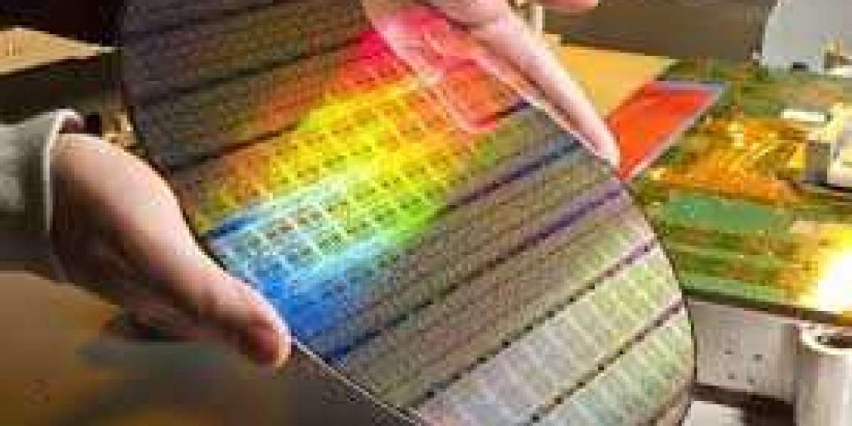
The semiconductor substrate marketplace is far from a homogenous entity; rather, it is a highly stratified ecosystem segmented by material composition, wafer diameter, and intended application architecture. Each specific segment requires distinct manufacturing techniques, raw materials, and quality assurance protocols, creating distinct operational sub-industries within the broader semiconductor fabric. For instance, the market for small-diameter wafers (150mm and below) remains active and highly profitable, catering primarily to legacy automotive components, basic discrete sensors, and specialized power modules that do not require advanced lithographic scaling. Conversely, the cutting-edge digital logic and memory markets are entirely dominated by 300mm pure silicon substrates, which demand absolute structural perfection and zero metallic contamination. Evaluating how these various product categories interact, shift, and compete requires an analytical breakdown of each Semiconductor Wafer Market segment to discern where capital allocation yields the highest return on investment.
Furthermore, material segmentation is increasingly defined by the operational boundaries of the end-use device. While elemental silicon remains the undisputed king for massive data processing and storage arrays due to its structural stability and cost profile, compound semiconductors are rapidly expanding their footprint. Gallium Arsenide (GaAs) and Indium Phosphide (InP) are critical for optoelectronic applications, such as laser diodes, fiber-optic communication components, and specialized solar cells used in space exploration. The growth dynamics within these material segments are independent of traditional consumer smartphone or PC lifecycles, often tied instead to macro-level infrastructure rollouts like satellite constellations or global telecom upgrades, providing a diversified revenue stream for agile substrate manufacturers.
What are compound semiconductors, and where are they primarily utilized? Compound semiconductors are made from two or more chemical elements, such as Gallium Arsenide (GaAs) or Indium Phosphide (InP), unlike traditional silicon wafers which consist of a single element. These compound materials exhibit unique optical and electrical properties, such as direct bandgaps, making them highly efficient for emitting and detecting light in fiber-optic communications, laser diodes, and advanced radar systems.
Why do legacy applications continue to use smaller wafer diameters like 150mm? Legacy applications like basic industrial sensors, simple automotive switches, and power regulators use mature circuit designs that do not benefit from advanced nanometer scaling. The tooling and machinery for 150mm wafers have long been fully depreciated financially, making the production of these simple chips extremely cost-effective on smaller wafers, as upgrading to larger diameters would require unjustifiably expensive capital reinvestment.
➤➤➤Explore MRFR’s Related Ongoing Coverage In Semiconductor Industry:
Building Automation System Market
Automatic Gate And Door Opening System Market